5.5. Dead-time Compensation
5.5.1. Overview
Dead time is the delay during a PWM cycle in which gate drive signals for both high-side and low-side transistors are inactive. This presents itself as a voltage distortion of roughly fixed amplitude and depends on the direction of phase current. In field-oriented control, this voltage distortion repeats six times per electrical cycle, with short transients near each zero-crossing of phase current.
Dead-time compensation in MCAF can be used to counteract some of the dead-time distortion, both in the current control loop itself, and in the feedback signals used in position and velocity estimators.
5.5.2. Definition and origin of dead time
Drive electronics for a three-phase PMSM includes a three-phase bridge shown in Figure 5.69.

Figure 5.69 Three-phase bridge, consisting of three half-bridges driving motor terminals A, B, and C. Each half-bridge has a high-side and low-side transistor that can connect the corresponding motor terminal to either the positive or negative end of the DC link.
The dead time is shown in Figure 5.70, expressed as a fraction \(\delta_1\) of the total PWM period \(T_\text{PWM}\). It is used to accommodate the time needed for switching transitions, and allow one transistor to turn off completely before the other starts turning on. This avoids shoot-through, where a temporary short-circuit occurs across the DC link and causes high power dissipation in both transistors.

Figure 5.70 An example of gate drive signals for one of the motor’s half bridges
The signals in Figure 5.70 are described below.
- Signal G is a raw generated pulse waveform with duty cycle \(D\).
- Signal H is the gate drive signal for the high-side transistor, which is active for duty cycle \(D-\delta_1\).
- Signal L is the gate drive signal for the high-side transistor, which is active for duty cycle \(1-(D+\delta_1) = 1-D-\delta_1\).
When G turns on, the low-side gate drive L turns off instantly, but the high-side gate drive H is turned on after a delay of dead time \(\delta_1T_\text{PWM}\). When G turns off, the high-side gate drive H turns off instantly, but the low-side gate drive L is turned on after a delay of dead time \(\delta_1T_\text{PWM}\).
5.5.3. Dead-time distortion
5.5.3.1. Output voltage during dead time
Field-oriented control in MCAF uses average-value modeling. The control variables can be represented by the mean value over the sampling time, and the sampling time consists of a discrete number of half-periods. MCAF R1 - R6 all use a sampling time of 1 full PWM period. The mean output voltage of the half bridge during a PWM cycle is \(D'V_{dc} = (D+\delta)V_{dc}\) where \(D'\) is the effective duty cycle, \(D\) is the desired duty cycle, and \(\delta\) is the effective duty cycle error. This error is caused by the dead time, and it is known as dead-time distortion.
During dead time, each half-bridge output is effectively in a high-impedance state, with voltage clamps at the DC link voltage rails from the freewheeling diodes of the power stage. (MOSFETs have intrinsic body diodes; IGBTs do not, and require anti-parallel diodes)
This causes the output voltage during dead time to vary, depending on the output current. In a motor drive, the half-bridge load is inductive, so the output voltage is one of the following, as shown in Figure 5.71:

Figure 5.71 Output voltage of a half-bridge with inductive load during dead time. Delay times \(t_\textrm{off}\) and \(t_\textrm{on}\) represent the propagation delay between the edge of the gate drive signal, and the moment the transistor voltage starts to change.
- If the output current is strictly positive (flowing out of the half bridge) during dead time, then the low-side free-wheeling diode turns on, and the output voltage is \(-V_d\), namely a diode drop below the negative terminal of the DC link, as shown by the green curve in Figure 5.71.
- If the output current is strictly negative (flowing into of the half bridge) during dead time, then the high-side free-wheeling diode turns on, and the output voltage is \(V_{DC}+V_d\), namely a diode drop above the positive terminal of the DC link, as shown by the black curve in Figure 5.71.
- If the output current reaches zero during the dead time, then the half-bridge undergoes discontinuous conduction, and the voltage is determined by interaction of the inductive load with the parasitic capacitance \(C_p\) and leakage resistance \(R_l\) of the half-bridge. This can lead to voltage oscillations at frequency \(f \approx 1/(2\pi\sqrt{L_sC_p})\), as shown by the red and orange curves in Figure 5.71. The exact waveform is hard to predict, and very sensitive to slight changes in output current.
Figure 5.72, Figure 5.73, and Figure 5.74 show oscilloscope traces captured to illustrate the effect of dead time on the dsPICDEM® MCLV‑2 Development Board running at 24Vdc, at 1 μs/division timebase and 10 V/division on the phase voltage measurement.
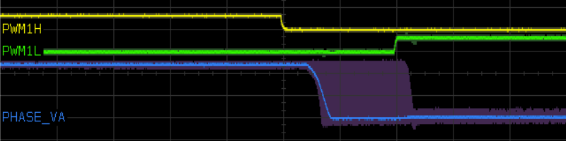
Figure 5.72 Output voltage behavior during dead time, falling transition on phase voltage output. Faint purple indicates persistence over many captured traces.
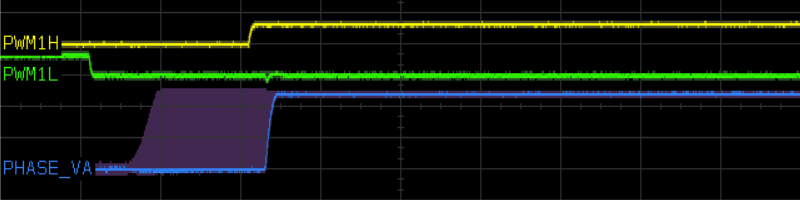
Figure 5.73 Output voltage behavior during dead time, rising transition on phase voltage output. Faint purple indicates persistence over many captured traces.
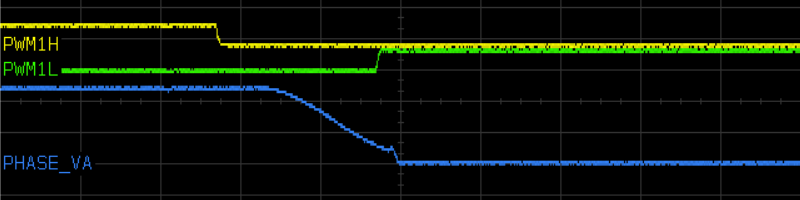
Figure 5.74 Output voltage behavior during dead time, falling transition on phase voltage output for current near zero.
5.5.3.2. Analysis of error bounds
The mean voltage over the sampling time can be bounded by looking at the upper and lower bounds caused by high positive and high negative currents during dead time. These are the green and black curves in Figure 5.71; similar curves are shown in Figure 5.75 labeled with effective duty cycles \(D' = D + \delta\).

Figure 5.75 Effective duty cycle over an entire PWM period
The major term in effective duty cycle error is just \(\delta = \plusmn\delta_1\) caused directly by dead time at currents which are not near zero. There are a few secondary effects:
- Diode drop voltage \(V_d\) during dead time — the resulting error tends to be very small: for example, a 1-volt drop on a 24-volt system during a total dead time of 4% of the entire PWM cycle represents an effective duty cycle error of 4% / 24 = 0.17%. It affects very low voltage systems most severely, but these are also cases where dead time can usually be reduced. Furthermore, since its effect is proportional to dead time, it can be lumped into an effective dead time \(\delta_1' \approx \delta_1 (1+V_d/V_{dc})\)
- Asymmetry in turn-on and turn-off times — this is shown in Figure 5.75. It effectively lengthens the dead time by the difference between turn-on and turn-off times, since turn-off in a well-designed motor drive is usually faster than turn-on — although it could also reduce the effective dead-time if turn-off is slower than turn-on. This appears to be the case in the oscilloscope traces captured in Figure 5.72 and Figure 5.73: the time span of output voltage transitions is smaller than the dead time. This effect can also be lumped into an effective dead time \(\delta_1' \approx \delta_1 + (t_\textrm{on} - t_\textrm{off})/T_\textrm{PWM}\).
- Discontinuous conduction — this is discussed in the next section.
5.5.3.3. Behavior during discontinuous conduction
When currents are near zero and the half-bridge enters discontinuous conduction, the effective duty cycle error \(\delta\) is between the upper and lower bounds \(\delta=\plusmn\delta_1\), and is a function of current that is difficult to model.
Equation 5.52 isolates the interesting behavior for currents \(|I| < I_\delta\) near zero, in a nonlinear function \(f_{nl}(u)\), which is some difficult-to-model empirical nonlinear function that maps the input range [-1,1] into the output range [-1,1]. In most cases, there is no need to know what it really is; some examples of nonlinear functions \(f_{nl}(u)\) are shown in Figure 5.76. The dead-time compensation in MCAF just assumes a linear function \(f_{nl1}(u) = u\).

Figure 5.76 Examples of nonlinear functions \(f_{nl}(u)\) varying in their behavior within the range \(|u| < 1\), including the sign function, the identity, a sigmoid function, and a constant.
The magnitude of current \(I_\delta\) under which discontinuous conduction is possible is approximately equal to the current ripple. Its behavior is within the discontinuous conduction zone is dependent on the relative magnitudes of \(I_\delta\) and characteristic current \(I_C = C_pV_{dc}/\delta_1T_\textrm{PWM}\) required to charge the parasitic capacitance \(C_p\). Reference [3] discusses both effects in detail.
5.5.3.4. Dead-time distortion voltage in field-oriented current control
The preceding sections have applied to a single half-bridge with inductive load. In field-oriented current control of a three-phase motor, the transformation of the dead-time voltage distortion into the synchronous (dq) frame is of interest, since this is the disturbance “seen” by the motor.
Figure 5.77 shows the unit voltage disturbance \(s\) in various reference frames, assuming sinusoidal currents and smooth angular rotation, and neglecting the discontinuous conduction zone.
From top to bottom:
- \(I\) — phase currents with some amplitude \(I_0\)
- \(s_A, s_B, s_C\) — sign of the corresponding current, with amplitude \(\plusmn 1\)
- \(s_{\alpha\beta}\) — sign vector in stationary (αβ) frame; \(s_\alpha = \frac{1}{3}(2s_A - s_B - s_C),\;s_\beta = \frac{1}{\sqrt{3}}(s_B - s_C)\). This represents a constant amplitude of \(\frac{4}{3}\) and an angle that jumps by 60° at each zero-crossing of current.
- \(s_{dq}\) — sign vector in synchronous (dq) frame; \(s_d = s_\alpha \sin \theta_e - s_\beta \cos \theta_e,\;s_q = s_\alpha \cos \theta_e + s_\beta \sin \theta_e\)

Figure 5.77 Unit voltage disturbances from dead-time distortion. Per-phase components \(s_A, s_B, s_C\) are shown, along with unit voltage disturbances \(s_{\alpha\beta}\) in the stationary reference frame, and \(s_{dq}\) in the synchronous reference frame.
Both d- and q-axis disturbances follow sinusoidal waveforms every 60° electrical angle. If the current vector is along the q-axis, then the unit d-axis disturbance \(s_d\) is centered around an angular disturbance of zero, with no DC offset. The unit q-axis disturbance \(s_q\) is centered around 90°, with smaller variation and a nonzero offset. For a unit dead-time distortion amplitude on each half-bridge, relevant characteristics of these waveforms are listed in Table 5.6.
| Characteristic | Value |
|---|---|
| D-axis peak disturbance | \(2/3\) |
| D-axis RMS disturbance | \(\sqrt{\frac{8}{9} + \frac{4\sqrt{3}}{3\pi} - \frac{16}{\pi^2}}\approx\) 0.05343 |
| Q-axis peak disturbance | \(4/3\) |
| Q-axis mean disturbance | \(4/\pi\approx\) 1.27324 |
| Q-axis RMS disturbance | \(\sqrt{\frac{8}{9} - \frac{4\sqrt{3}}{3\pi}} \approx\) 0.39215 |
If the current vector contains a d-axis component, as in the flux control algorithms, then the dead-time disturbance will be centered around the direction of the current vector, instead of around the q-axis.
These are the effects of unit voltage disturbances. In a real system, the voltage disturbance when the current magnitude is large (avoiding discontinuous conduction) are \(-\delta_1 V_{dc} s\) in each reference frame. In other words:
- In the stationary frame, the dead-time voltage disturbance is \(-\delta_1 V_{dc} s_{\alpha\beta}\) with amplitude \(\frac{4}{3}\delta_1 V_{dc}\)
- In the synchronous frame, the dead-time voltage disturbance is \(-\delta_1 V_{dc} s_{dq}\), also with amplitude \(\frac{4}{3}\delta_1 V_{dc}\), but sweeping across an arc within ±30° of the current vector. Peak, mean, and RMS disturbances in the dq reference frame can also be computed proportionally, so that a 4% dead time (2 μs for each transition in a 50 μs PWM period) with a 24V DC link and a current vector along the q-axis should experience a mean q-axis disturbance of approximately 0.04 × 24 × 1.27324 = 1.22231V.
The voltage disturbances from dead-time distortion may also be visualized as an x-y plot (α-β or d-q). Figure 5.78 shows such plots in the case of a PMSM in the motoring quadrant. In the stationary frame, dead-time distortion maps a circular voltage trajectory into 6 disconnected arcs that look something like a sawblade. In the synchronous frame, dead-time distortion maps a single point, representing constant dq voltage, to a small arc with a mean DC offset along the q-axis that subtracts from the desired voltage.
In the generating quadrant, the direction of voltage disturbance would be reversed and would cause a mean DC offset along the q-axis that adds to the desired voltage.

Figure 5.78 Voltage disturbances from dead-time distortion in stationary (αβ) frame (left) and synchronous (dq) frame (right). This case represents large phase currents (so that discontinuous conduction can be neglected) with a desired voltage of some amplitude \(V_1\) that leads the current by 30° electrical, and a product \(\delta_1 V_{dc}\) (product of dead time fraction and DC link voltage) that is \(0.15V_1\). In this case, the disturbance in the αβ and dq frames has amplitude \(\frac{4}{3}\delta_1 V_{dc} = \frac{4}{3}\times 0.15V_1 = 0.2V_1\).
5.5.4. Practical effects of dead-time distortion
There are two main areas in which dead-time distortion is detrimental to motor control:
- effect on current control
- effect on position and velocity estimators
5.5.4.1. Dead-time distortion and field-oriented current control
In FOC, the current controllers operate in the synchronous (dq) reference frame. Dead-time distortion causes a voltage disturbance to the current controllers at \(6f_e\) (six times the electrical frequency) that occurs around each zero-crossing of phase current.
At low velocity, the current controllers will eventually regain zero steady-state error after each transient. The disturbance shown on the right of Figure 5.78 must be counteracted by an increase in voltage of opposite sign:
- The average reduction in q-axis voltage at the motor must be canceled by the q-axis current controller increasing its voltage by the same amount
- The d-axis disturbance, roughly a linear ramp, must be canceled by the d-axis current controller with a change in controller output in the opposite direction.
At high velocity, the changes in output voltage required to counteract the dead-time voltage distortion occur fast enough and often enough that the current controllers are unable to cancel the distortion completely.
Figure 5.79 shows measured and predicted voltage requirements for the Nidec Hurst DMA0204024B101 at low velocity (about 240RPM) and various dead times, driven with the dsPICDEM® MCLV‑2 Development Board, and running with a smooth, light load that requires \(I_q \approx\) 0.5 A. The left-hand graph shows the stationary-frame output voltage \(V_{\alpha\beta}\). The red circle is the back-emf magnitude. The blue, orange, and green scatter plots show measured samples of αβ-frame voltage at 1, 2, and 3 microsecond dead-times. Black dots mark the predicted output voltage based on a pure signum function \(f_{nl0}(u)\) (see Figure 5.76) and essentially show the six 60° sectors of the back-emf circle “exploding” outwards due to the extra voltage required to counteract dead-time distortion. These match the measured data fairly well, at least when not in discontinuous conduction. The gain of the dead-time distortion in the measured data is slightly greater than predicted (note that the blue, orange, and green hexagonal scatter plots lie slightly outside the black arcs) and may be due to the diode voltage drops mentioned in Section 5.5.3.2.
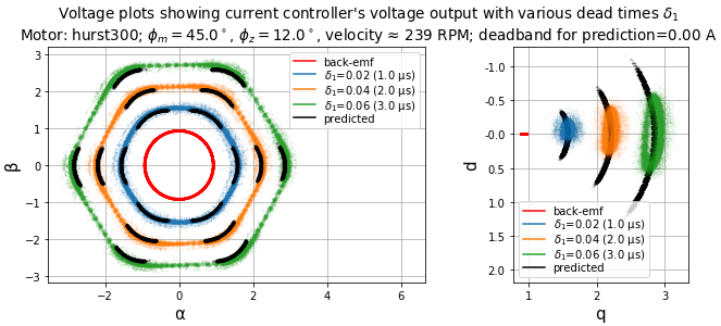
Figure 5.79 Voltage plots in stationary and synchronous frames for various dead times.
The right-hand graph of Figure 5.79 shows the same information in the synchronous (dq) frame, where the back-emf is a tight cluster, varying very slightly along the q-axis due to small velocity fluctuations. The measured and predicted data for \(V_{dq}\) approximately follow arcs showing the increase in q-axis voltage and the sweep in d-axis voltage.
Figure 5.80 shows the same measured voltages, but with a change in the predicted voltage that takes discontinuous conduction into account, by using a linear model \(f_{nl1}(u) = u\) for \(u = I/I_\delta\) within the range \(|I| < I_\delta\) to handle behavior near the zero crossings (see Figure 5.76). The zero-crossing range used in this graph is \(I_\delta\) = 0.12A.
Note the improved match in both stationary and synchronous frames, compared with Figure 5.79.
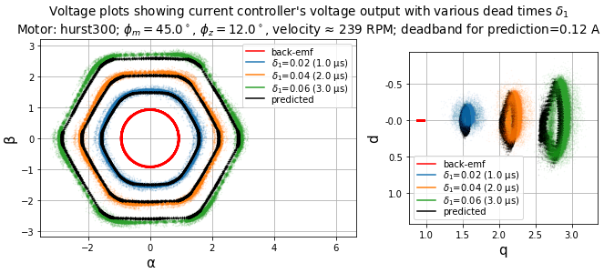
Figure 5.80 Voltage plots in stationary and synchronous frames for various dead times.
The current itself is shown in Figure 5.81. Measured current tracks the intended circular trajectory in the stationary frame (constant current \(I_q\) in the synchronous frame) fairly well, degrading slightly as the dead time is increased.
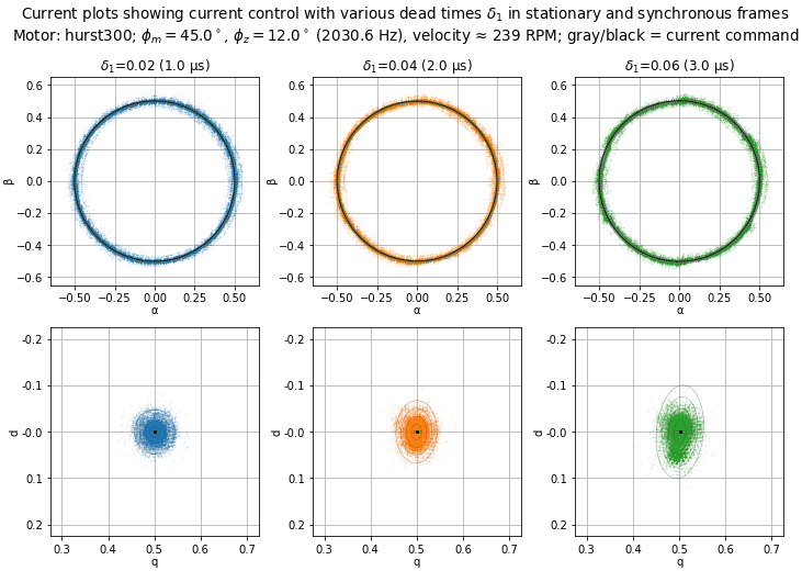
Figure 5.81 Current plots in the stationary (αβ) and synchronous (dq) frames
for various dead times. The black circle (in the αβ frame)
and dot (in the dq frame) represent average q-axis reference current; these are
shown directly on top of the
gray circle (αβ frame) and bar (dq) that represent
the measured q-axis reference current, which fluctuates slightly with
velocity and load changes.
The faint concentric gray ellipses in the dq frame
are error ellipses,
based on the covariance of the measured currents,
at 1, 2, 3, and 4 standard deviations from the mean.
(For purely random noise from a normal distribution,
the expected fraction of data enclosed by error ellipses
follows the cumulative distribution function (CDF) of a
chi-squared distribution
with two degrees of freedom, \(\chi^2(2)\).
Approximately 39.35% of samples are expected to lie within 1 standard deviation;
86.47% within 2 standard deviations, 98.89% within 3 standard deviations,
and 99.96% within 4 standard deviations.)
The effects of dead-time distortion change as velocity increases. Figure 5.82, Figure 5.83, Figure 5.84, and Figure 5.85 show the same 10-pole motor and current control tuning at 1200 RPM and 1800 RPM.
At these velocities, the sixth-harmonic frequency is 600 Hz and 900 Hz, respectively. Both are below the current control bandwidth (2031 Hz in this case), but not by much, and the result is an increase in current distortion.
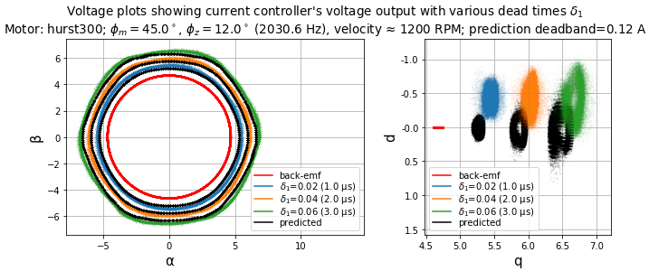
Figure 5.82 Voltage plots in stationary and synchronous frames for various dead times.
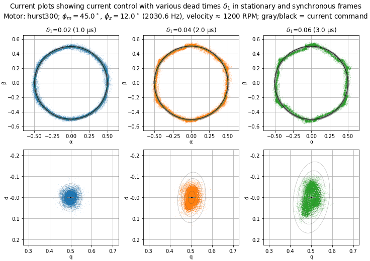
Figure 5.83 Current plots in the stationary and synchronous frames for various dead times. (See Figure 5.81 for more information about this type of graph.)
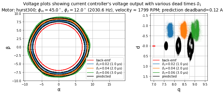
Figure 5.84 Voltage plots in stationary and synchronous frames for various dead times.
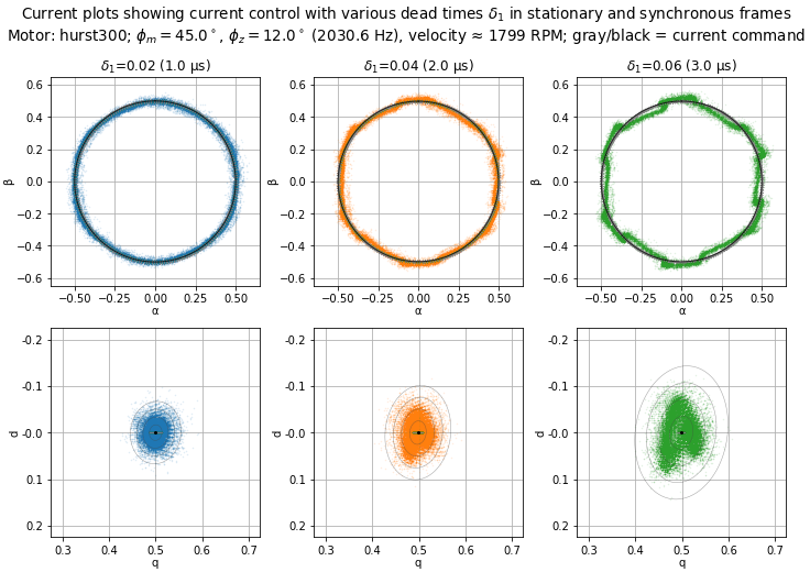
Figure 5.85 Current plots in the stationary and synchronous frames for various dead times. (See Figure 5.81 for more information about this type of graph.)
The DC voltage offset in \(V_{dq}\) visible in Figure 5.82 and Figure 5.84 (the shift between predicted and measured voltage) is probably due to these three effects:
- resistive voltage drop — \(IR \approx\) 0.19V along the q axis
- inductive voltage drop — \(I\omega_e L \approx\) 0.11V at 1200 RPM, 0.17V at 1800 RPM, along the d axis
- sample input-to-output delay — \(\omega_e T_d\) for \(T_d = 1.5T_s =\) 75 μs is about 2.7° at 1200 RPM and 4.1° at 1800 RPM. At 1200 RPM, with a 2.7° rotation of a 6 V signal along the q axis we can expect a d-axis shift of ≈ 0.28 V. At 1800 RPM, with a 4.1° rotation of an 8.2 V signal along the q axis, we can expect a d-axis shift of ≈ 0.58V
The total resulting voltage shifts are consistent with the figures.
5.5.4.1.1. Dead-time distortion with low-bandwidth current controllers
We can take similar measurements for a low-bandwidth current controller. Figure 5.86 and Figure 5.87 are with the same motor (Nidec Hurst DMA0204024B101) using the default current loop tuning in motorBench® Development Suite. With this tuning, the current loop bandwidth is around 235 Hz. These tests show operation at 240 RPM with a smooth light load of ≈ 0.5 A.
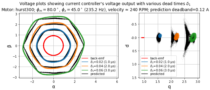
Figure 5.86 Voltage plots in stationary and synchronous frames for various dead times.
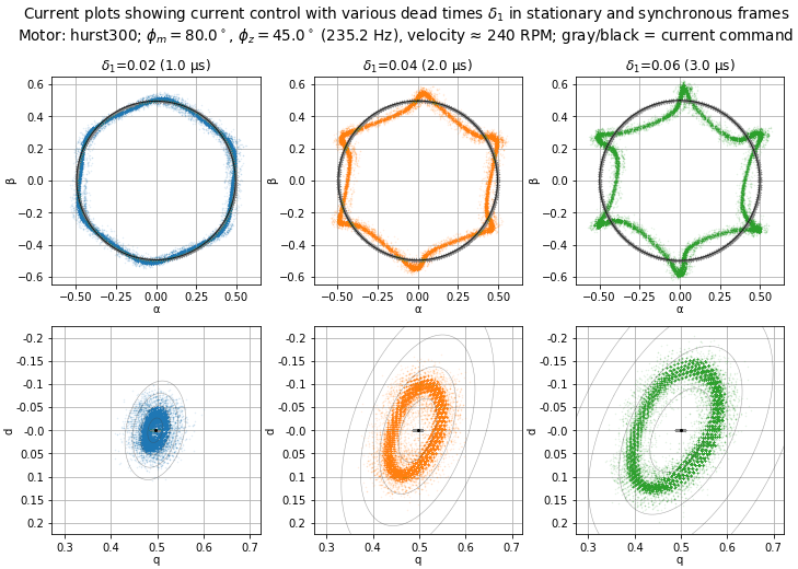
Figure 5.87 Current plots in the stationary and synchronous frames for various dead times. (See Figure 5.81 for more information about this type of graph.)
The result is a much higher current distortion even at the low electrical frequency of 20 Hz; The dead-time distortion frequency \(6f_e =\) 120Hz is about half the current loop bandwidth.
Figure 5.88 and Figure 5.89 show operation at 600 RPM (50 Hz electrical frequency, \(6f_e =\) 300 Hz) with a smooth light load of ≈ 0.5 A. In this case, the disturbance frequency is above the current loop bandwidth, and the current loop can barely react to the dead-time distortion — note that the voltage outputs in the synchronous frame are fairly tightly-clustered spots in the graphs, and in the stationary frame are almost circular.
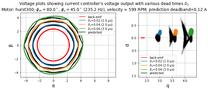
Figure 5.88 Voltage plots in stationary and synchronous frames for various dead times.
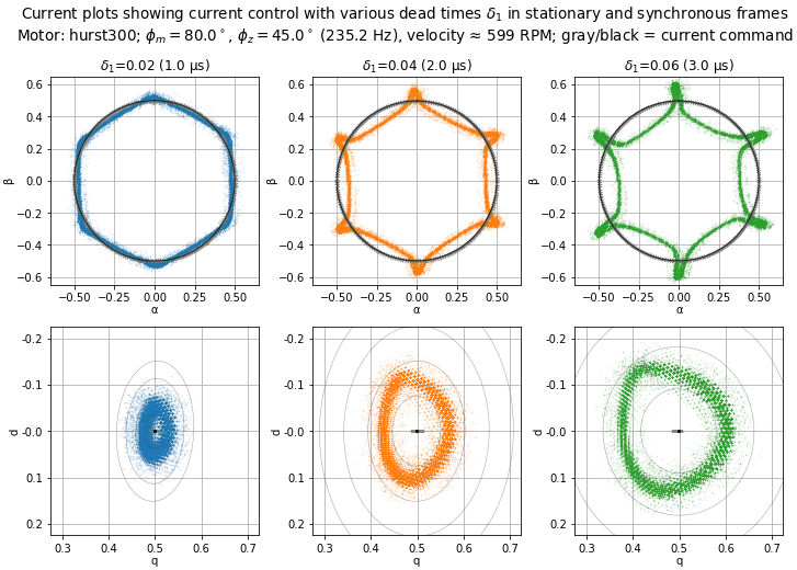
Figure 5.89 Current plots in the stationary and synchronous frames for various dead times. (See Figure 5.81 for more information about this type of graph.)
Figure 5.90 and Figure 5.91 show operation at 1200 RPM (100 Hz electrical frequency, \(6f_e =\) 600 Hz) with a smooth light load of ≈ 0.5 A. In this case, the disturbance frequency is even further above the current loop bandwidth. Again, the current loop can barely react to the dead-time distortion — note that the voltage outputs in the stationary frame are almost circular, and in the synchronous frame are fairly tightly-clustered, although with some fluctuations mostly along the d-axis, which is indicative of angle jitter, perhaps due to the torque ripple causing velocity fluctuations.
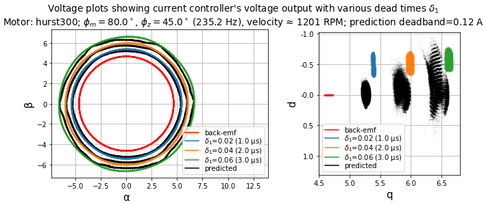
Figure 5.90 Voltage plots in stationary and synchronous frames for various dead times.
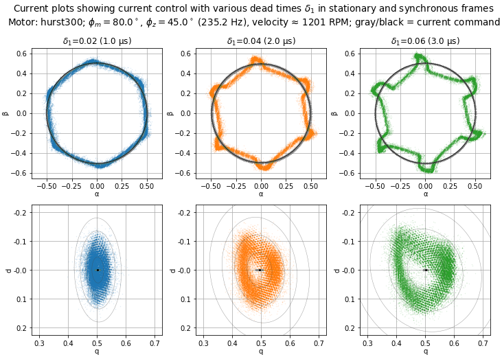
Figure 5.91 Current plots in the stationary and synchronous frames for various dead times. (See Figure 5.81 for more information about this type of graph.)
There are a number of reasons for tuning a current loop with a more aggressive bandwidth, and improving otherwise poor performance in the presence of dead-time distortion is one of them.
5.5.4.2. Dead-time distortion and sensorless estimation
Position and velocity estimators based solely on voltage and current measurements are sensitive to errors in the voltage and currents. These typically try to estimate a back-emf voltage vector and track its angle. Since dead-time distortion causes voltage errors between the current controller outputs and the actual voltage present on the motor terminals, these estimators tend to produce significant errors when the back-emf voltage is below the dead-time distortion voltage amplitude \(\frac{4}{3}\delta_1 V_{dc}\).
Most sensorless estimators are less sensitive to q-axis voltage errors, which affect only the amplitude of the estimated back-emf vector once the estimator has locked onto it), and more sensitive to d-axis voltage errors, which perturb the angle of the estimated back-emf vector.
The AN1292 PLL also relies on the amplitude of the estimated back-emf, so it is likely more sensitive to dead-time distortion than other estimators.
Dead-time compensation can improve the performance of sensorless estimators at low velocities, by correcting the estimated back-emf for the effects of dead-time distortion.
5.5.5. Dead-time compensation
There are three main methods for mitigating dead-time distortion, roughly in order of priority:
- Reduce the dead time. This may be possible with careful gate drive design and testing. Note: do not assume that dead time is adequate based only on testing one sample of a motor drive board at room temperature! Attempts to minimize the dead time, while still protecting against shoot-through, require a detailed understanding of the switching transient’s sensitivity to temperature, duty cycle, current, and part-to-part variation of the transistors and the gate drive circuitry.
- Increase the current loop bandwidth. This inherently compensates for dead-time distortion, at least at electrical frequencies below the current loop bandwidth. As discussed above, low-bandwidth current control loops are unable to counteract the effects of dead-time distortion.
- Add voltage compensation. Although this is the least desirable of the three methods, it can potentially reduce the effects of dead-time distortion.
5.5.5.1. MCAF per-phase dead-time compensation algorithm
The voltage compensation method available in MCAF is based on per-phase estimates of the dead-time distortion voltage, added to the forward path of the current control loop, and the feedback path of the position and velocity estimator. This is known as the “per-phase” method and can be selected in the Customize page of motorBench® Development Suite.
A block diagram of the dead-time compensation module dtcomp is shown in
Figure 5.93, and in context in Figure 5.92.
The inputs to this block are phase currents \(I_{abc}\)
and duty cycles \(D_{abc2}\) that are outputs of the ZSM block.

Figure 5.92 Dead-time compensation in MCAF, in context of the main FOC block diagram.

Figure 5.93 Per-phase dead-time compensation in MCAF.
The upper half of the dead-time compensation block, above the dashed line shown in Figure 5.93, handles the feedback voltage for use by position and velocity estimators. The duty cycles are converted to the stationary (αβ) frame using a Clarke transform, and then delayed by two cycles to match the current sampling delay (TBD add link here). Dead-time compensation vector \(\Delta D_{\alpha\beta f}\), which is a duty cycle vector in the stationary frame, is added to the delay-matched duty cycle and then multiplied by DC link voltage \(V_{dc}\) to compute the estimator feedback voltage \(V_{\alpha\beta f}\).
The lower half of the dead-time compensation block shows the core of the dead-time compensation algorithm, which has three portions:
- Computation of estimated unit disturbance signals \(\hat{s}_{abc}\)
- Computation of feedback-path dead-time compensation vector \(\Delta D_{\alpha\beta f} = D_{\mathrm{fb}}\hat{s}_{\alpha\beta}\) from estimated unit disturbance signals \(\hat{s}_{\alpha\beta}\) in the stationary frame
- Computation of forward-path dead-time compensation vector \(\Delta D_{abc} = D_{\mathrm{fwd}}\hat{s}_{abc}\) as a per-phase set.
The per-phase unit disturbance signals are calculated as shown in Figure 5.93 using a saturation block with linear gain \(K = K_0/I_\delta\) for a chosen current amplitude \(I_\delta\) and fixed scaling factor \(K_0\), and limits \(\plusmn A = \plusmn 1\).
This effectively computes the nonlinear function \(f_{nl}(I/I_\delta)\), shown in Equation 5.53 and applied as Equation 5.54.
5.5.5.2. Behavior when disabled
If the “None” variant of dead-time compensation is chosen in the Customize page of motorBench® Development Suite, then the upper part of Figure 5.93 calculating estimator feedback voltages \(V_{\alpha\beta f}\) still executes, but compensation values \(\Delta D_{\alpha\beta f}\) and \(\Delta D_{abc}\) are set to zero.
5.5.5.3. Choice of parameters
Each of the three parameters may be adjusted:
- Current linearity range \(I_\delta\) as a fraction of fullscale current
- Forward-path gain \(\alpha_{\mathrm{fwd}} = D_{\mathrm{fwd}}/\delta_1\)
- Feedback-path gain \(\alpha_{\mathrm{fb}} = D_{\mathrm{fb}}/\delta_1\)
The forward and feedback gains are selected as a proportion of the expected dead time.
Note: The guidance in this section is preliminary and is based on available testing so far. Future work may help improve this guidance.
5.5.5.3.1. Current linearity range
Empirical work with the Nidec Hurst DMA0204024B101 motor and dsPICDEM® MCLV‑2 Development Board showed improved stability in the range of \(K \approx\) 133 – 200, corresponding to \(I_\delta = 0.01I_{fs}\) = 0.044 A to \(0.015I_{fs}\) = 0.066 A.
5.5.5.3.2. Forward-path gain
Forward-path dead-time compensation was not particularly successful. Use of nonzero forward-path gain is not recommended without performing detailed testing on the intended motor and load, to determine a desirable value.
An unloaded motor, which experiences very low q-axis currents, is a difficult subject to reduce the effects of dead-time distortion.
With the Nidec Hurst DMA0204024B101 motor, a forward-path gain of only \(\alpha_{\mathrm{fwd}} = 0.25\) produced the least distortion; increasing gain much beyond that point caused the distortion to increase again.
For the motor loaded with about 0.5 A q-axis current, the dead-time compensation was more effective, with \(\alpha_{\mathrm{fwd}} = 0.625\) producing the least distortion.
5.5.5.3.3. Feedback-path gain
Nonzero feedback-path gain was successful at improving estimator performance of the AN1292 PLL at very low velocities. Values of \(\alpha_{\mathrm{fb}} = 0.5\) were generally successful on several motors tested, and lowered the minimum operating speed by a factor of anywhere from 2 to 4.
If \(\alpha_{\mathrm{fb}}\) is too high, the motor controller tended to “clench” and apply full current. (This effect seems to be reduced if the motor resistance is underestimated intentionally by a few percent.)
Use of nonzero feedback-path gain with the AN1292 PLL is recommended, starting with a gain of 0.4 - 0.5. The gain may be increased, with careful experimentation to avoid the “clenching” behavior, to improve torque performance at low speed.
5.5.5.4. Experimental results
Some experimental data showing the improvement from feedback-path dead-time compensation is shown below in Figure 5.94.
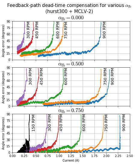
Figure 5.94 Per-phase dead-time compensation in MCAF.
In this case, the Nidec Hurst DMA0204024B101 and dsPICDEM® MCLV‑2 Development Board were used to show an increase in tolerable load current at lower speeds. The current loop was tuned to a high bandwidth (≈ 2 kHz) and the velocity loop was tuned to a low bandwidth (≈ 1.8Hz) to allow slowly-changing current. The AN1292 PLL estimator was used for commutation with quadrature encoder as an angle reference.
This was run at a variety of motor velocities for three different values of \(\alpha_{\mathrm{fb}}\), and a manually-applied load torque gradually increased until the encoder and estimators diverged by more than 60° electrical. As the commutation error approaches 90° electrical, torque production drops off rapidly and the motor undergoes cycle slip behavior.
Figure 5.94 shows an increase in motor current as \(\alpha_{\textrm{fb}}\) is increased, for a given velocity, before approaching a cycle slip. This increased motor current means the motor controller can apply a larger current with less commutation angle error, providing an improved torque response at low speeds.
5.5.5.5. Implementation notes
Fixed gain scaling factor \(K_0 = KI_\delta = 2\) since in MCAF, currents are represented with numerical full-scale of twice the ADC full-scale values to leave design margin for avoiding overflow. For example, on dsPICDEM® MCLV‑2 Development Board the full-scale ADC current is 4.4 A but the numerical full-scale range of currents is 8.8 A.
5.5.6. References
| [1] | R. B. Sepe and J. H. Lang, “Inverter nonlinearities and discrete-time vector current control”, IEEE Transactions on Industry Applications, vol. 30, no. 1, pp. 62-70, Jan/Feb 1994. |
| [2] | G. Pellegrino, P. Guglielmi, E. Armando and R. I. Bojoi, “Self-Commissioning Algorithm for Inverter Nonlinearity Compensation in Sensorless Induction Motor Drives”, IEEE Transactions on Industry Applications, vol. 46, no. 4, pp. 1416-1424, Jul/Aug 2010. |
| [3] | T. Mannen and H. Fujita, “Dead-Time Compensation Method Based on Current Ripple Estimation”, IEEE Transactions on Power Electronics, vol. 30, no. 7, pp. 4016-4024, Jul 2015. |