5.1.3. DC link compensation
Variability in the DC link voltage manifests itself as a time-varying gain of the power electronics block; if the DC link voltage increases by 10%, then for the same duty cycles applied to a three-phase bridge, the voltage output will also be increased by 10%.
This affects the behavior of a FOC motor controller in a few significant ways:
- Current controller loop gain changes proportionally to DC link voltage. This variation can degrade the stability of the current controller.
- Voltage transients in the DC link cause a disturbance to the current loop.
- Sensorless estimators that rely only on duty cycle signals will also see a gain shift proportional to DC link voltage.
We can compensate for DC link voltage by converting from voltage to duty cycle in the forward path, as shown in Figure 5.12.
Essentially the \(abc\) voltages coming out of the Inverse Clarke blocks are multiplied by the reciprocal of the DC link voltage and then used as the input of the zero sequence modulation (ZSM) block:
where the subscript \(abc0\) represents the unmodified three-phase output of the Inverse Clarke transform, prior to shifting and clipping by the ZSM block.
In addition, we need to make the output limits of the current controller scale proportionally to \(V_{dc}\), in order to reflect the physical limits of the three-phase bridge.
5.1.3.1. Transients
DC link compensation will work correctly in the presence of transients if the dynamics of sensing \(V_{dc}\) are much faster than the dynamics of the voltage transient itself.
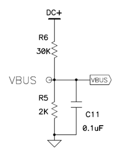
On the dsPICDEM® MCLV‑2 Development Board, for example, there is a 188 μs RC filter (see Figure 5.13) that dominates the dynamic behavior of sensing. This has a 3 dB bandwidth of about 847 Hz, so DC link compensation should be able to reject transients with frequency content significantly lower than this, and cannot reject transient content around or above this frequency. In general, motor drive designs should use RC filters with shorter time constants, typically on the order of 1-10 μs; antialiasing concerns are usually less important than avoiding excessive phase lag, because the DC link capacitors already limit high frequency content.

Figure 5.13 RC filter in MCLV-2
5.1.3.2. Implementation Notes
The reciprocal step of computing \(R_V = 1/V_{dc}\) in fixed-point relies on choosing a reasonable scaling factor. In the MCAF, we use Q12 representation with a scaling factor of \(1/V_{dcmax}\), which allows accurate computation of \(R_V\) over the voltage range \(\frac{V_{dc}}{V_{dcmax}} \in [1/8, 1]\). For the MCLV-2 board’s maximum input voltage range of 52.8 V, this allows accurate reciprocal calculations between 6.6 V and 52.8 V. For the MCHV-2 and MCHV-3 boards’ maximum input voltage range of 453.3 V, this allows accurate reciprocal calculations between 56.7 V and 453.3 V.
If \(V_{dc} < V_{dcmax}/8\) the reciprocal is clamped at its maximum value (32767 counts = \(7.99976/V_{dcmax}\)) and the DC link compensation will not be perfect; in this case the overall open-loop gain (including the gain of the three-phase bridge in hardware, and DC link compensation in software) will be less than one.
5.1.3.2.1. Feature support
DC link compensation was not present in MCAF R1 but has been added in MCAF R2.

