5.1.3. Current measurement
5.1.3.1. Overview
Current measurement algorithms take individual current measurements (phase currents, low-side transistor currents, or DC link currents) and adapt them for use in the feedback path of field-oriented control. This feedback processing step is shown as “gain/ofs compensation” in Figure 5.8.

Figure 5.8 Simplified FOC diagram
Current measurement includes several aspects:
run-time compensation of current offset error
compile-time compensation of current gain error, for cases such as the MCLV-2
use of single/dual/triple-channel current measurement
5.1.3.2. Gain and offset compensation
Gain and offset errors in current measurement are undesirable in a motor drive for several reasons. They cause unwanted torque ripple. Motor drives must be derated in current capacity to cover uncertainty in current-sense gain and offset, so that the components are kept within their safe operating area.
See ADC Calibration and Compensation for more information.
5.1.3.3. Current measurement channels
MCAF supports flexibility in the number of channels (“shunts”) that can be used. Typical current sensing for low-current [1] motor control uses shunt resistors placed in the lower leg(s) of the power stage, as shown in Figure 5.9.
In dual-channel and triple-channel measurement, phase currents are sensed through current sense resistors \(R_{sa}\), \(R_{sb}\), and \(R_{sc}\). Dual-channel requires two current sense channels, whereas triple-channel measurement requires all three.
In some cases, single-channel measurement (“single-shunt”) can be used, where one current sense resistor \(R_{s,dc}\) measuring the DC link current is enough to reconstruct phase currents.

Figure 5.9 Typical current sense resistors in a three-phase bridge
5.1.3.3.1. Current polarity conventions
MCAF uses the following convention for current polarity, as shown in Figure 5.9.
Phase currents \(I_a, I_b,\) and \(I_c\) are positive when current flows out of the bridge output terminals into the motor.
DC link current \(I_{dc}\) is positive when current flows into the positive DC link terminal and out the negative DC link terminal of the bridge.
As shown in Figure 5.9, positive phase currents correspond to negative values of phase shunt currents \(I_{sa}, I_{sb}, I_{sc}\).
5.1.3.3.2. Validity of lower-leg shunt resistors
As shown in Figure 5.9, shunt resistor \(R_{sa}\) measures current \(I_{sa}\), which equals \(-I_a\) as long as the lower transistor QAL has been turned on.
This has several minor disadvantages:
The low-side transistors must be turned on long enough for any transients to settle, so that the ADC can obtain a good sample of currents. (This usually isn’t a big deal, especially if bootstrap gate drives are used, where the low-side transistors need to be turned on enough to recharge bootstrap capacitors.)
Required signal bandwidth of signal conditioning is much greater than the bandwidth of interest of the phase currents; usually at least 500 kHz so the settling time is small and the low-side transistor on-time can be short. The op-amps used for signal conditioning must have an appropriate gain-bandwidth product (GBWP) to support this, for example 10 MHz GBWP for a gain of 20, in order to reach a signal bandwidth of 500 kHz.
Gate charge current conducts through the shunt resistors, so during turn-on and turn-off, the voltages across the current sensor experience additional spikes
The required voltage across the shunt resistors takes away some of the available voltage needed to turn on the low-side transistors. Make sure there is sufficient gate voltage remaining to guarantee the low-side transistors are fully on when the drive is operating at its highest rated output currents — which is also when full transistor turn-on is needed the most.
5.1.3.3.3. Triple-channel current measurement
When all three phase currents are measured, this maximizes the signal-to-noise ratio. It also adds some redundancy: \(I_{sa} + I_{sb} + I_{sc}\) should be near zero when all low-side switches are turned on.
This configuration is recommended for the most noise-sensitive applications.
In this case, a full 3×2 Clarke transform is used.
5.1.3.3.4. Dual-channel current measurement
Two phase currents are enough to reconstruct the third current, assuming that \(I_{sa} + I_{sb} + I_{sc} = 0\). This does give up redundancy, and the overall noise level is increased.
In this case, a reduced 2×2 Clarke transform is used.
With dual-channel measurement, gain errors between the current sense channels manifest themselves as a cross-coupling effect in the phase that is sensed directly; suppose \(I_{sa}\) is 10 A, \(I_{sb}\) is -10 A, and \(I_{sc}\) is zero, but phase A’s gain is +5%, phase B’s gain is -5%, and phase C not measured. Then the sensed values of current are 10.5 A, -9.5 A, and -1 A.
5.1.3.3.5. Single-channel current measurement
The single channel current algorithm is used to reconstruct the three phase currents by measuring the DC link current. With the knowledge of switching states and the DC link current, the three phase motor currents are reconstructed as shown in Figure 5.10. Based on the switching state, either the upper transistors or the lower transistors must include only one phase’s transistor that is turned on, which allows estimation of that phase current from the DC link current.
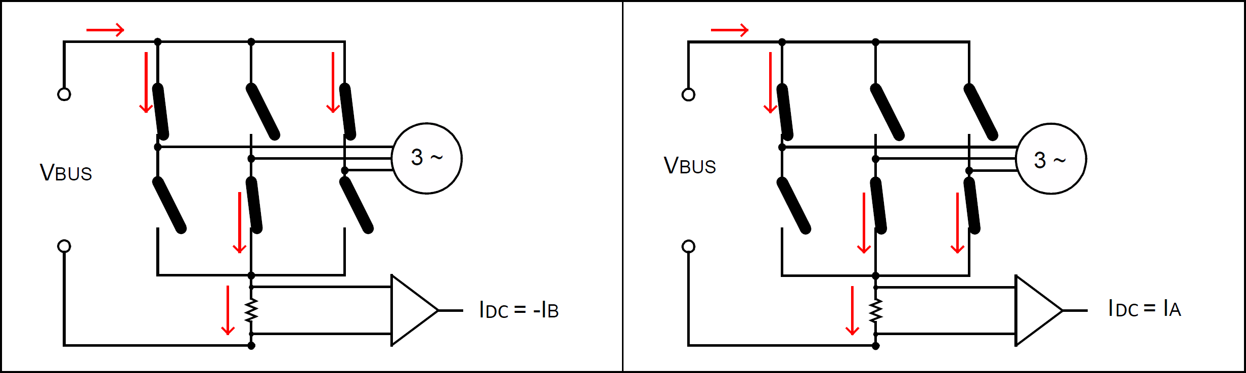
Figure 5.10 Instances of current reconstruction: Left image: \(I_B = -I_{DC}\) (DC link current flows out of motor and through lower leg of phase B). Right image: \(I_A = I_{DC}\) (DC link flows through upper leg of phase A and into motor).
If the phase currents are reconstructured using single channel without adjusting the duty cycles, the outputs from Zero Sequence Modulation (ZSM) can result in three-phase currents which are distorted and poses a challenge to perform FOC. This happens due to less time to sample currents using single shunt in the low-modulation index region, and sections of mid-to-high modulation index regions.
This is resolved by adjusting the ZSM outputs to meet the minimum time window requirements, resulting in better (sinusoidal) current information. Here, we need to ensure sufficient time for each active vector to sample current through the single channel. To achieve this, we check for active vector against a minimum time window \(t_{\rm sample}\), and compensate if required. The minimum time window can be adjusted in the Customize page of motorBench® Development Suite.
In the use case shown below in Figure 5.11, the time window T2 is not wide enough to sample current through the single channel. In order to allow a minimum time window for current measurement, we modify this time. The active vector time T2 is increased to meet the minimum time window, and the same is compensated in the falling edge (second half of PWM cycle).
This adjustment is not needed if the active vector time T2 is wide enough for the current measurement to be valid and accurate.
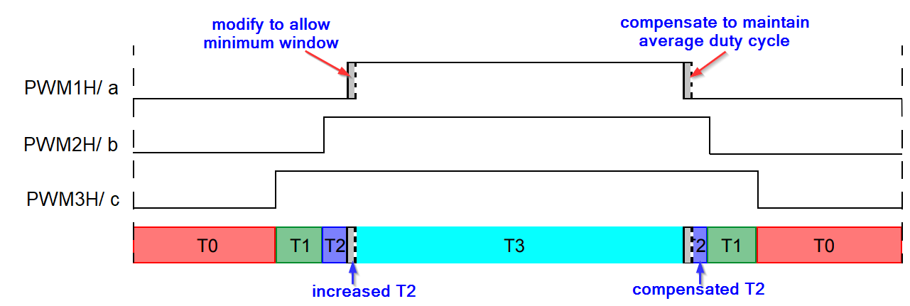
Figure 5.11 Duty cycle time T2 being adjusted
When the outputs (duty cycles) are modified in the first half of PWM cycle, they are also compensated on the falling edge during its second half of the PWM cycle. This ensures the average voltage vectors (duty cycles) remain the same.
On some boards where the delays due to gate driver propagation and opamp slew rate are larger, the ADC trigger delay \(t_{\rm delay}\) will need to be adjusted to meet the delay requirements. The ADC trigger delay can be adjusted in the Customize page of motorBench® Development Suite.
For more information on implementation details of single channel based current reconstruction for FOC, see Microchip’s application note AN1299.
5.1.3.3.6. Microchip development board support
Microchip motor control development boards supported by motorBench are listed in the following table, with current polarities (as seen by the ADC) shown: a green plus indicates positive polarity, and a blue minus indicates negative polarity. Blank table cells mean the specified current input is not sensed.
Board |
\(I_a\) |
\(I_b\) |
\(I_c\) |
\(I_{dc}\) |
Comments |
|---|---|---|---|---|---|
|
|
|
|||
|
|
|
|||
dsPIC33CK Low Voltage Motor Control (LVMC) Development Board |
|
|
|
|
|
|
|
|
|
5.1.3.3.7. Implementation notes
Support history:
Number of channels |
single |
dual |
triple |
Comments |
|---|---|---|---|---|
MCAF R1 – R6 |
|
Dual includes phases A and B only. |
||
MCAF R7 |
|
|
|
Dual includes phases A and B only. |