7.3. MCLV-2 Sense Resistors
The dsPICDEM® MCLV‑2 Development Board contains a three-phase bridge with low-side 25 mΩ shunt resistors for current sense circuitry on the A and B legs of the bridge as well as in the DC current path, as shown in Figure 7.1. Voltages across the sense resistors are used to sense currents \(I_a\), \(I_b\), and \(I_{dc} = I_a + I_b + I_c\).
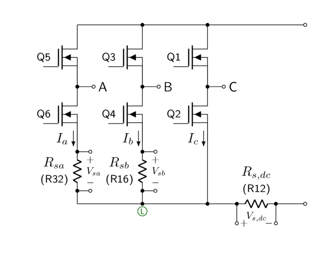
Figure 7.1 Three-phase bridge in MCLV-2, ideal circuit
In a real circuit board, the current trace at node Ⓛ connecting the A, B, and C legs of the bridge is not uniform in voltage, because it contains nonzero voltage drops along parasitic resistance of the trace. In the MCLV-2 board, this resistance can be modeled as three series resistors \(R_{p1}\), \(R_{p2}\), and \(R_{p3}\), in Figure 7.2. Kelvin connections are made directly from the sense resistor terminals to a differential amplifier, so that the voltage drops along these parasitic resistances do not affect the current measurements.
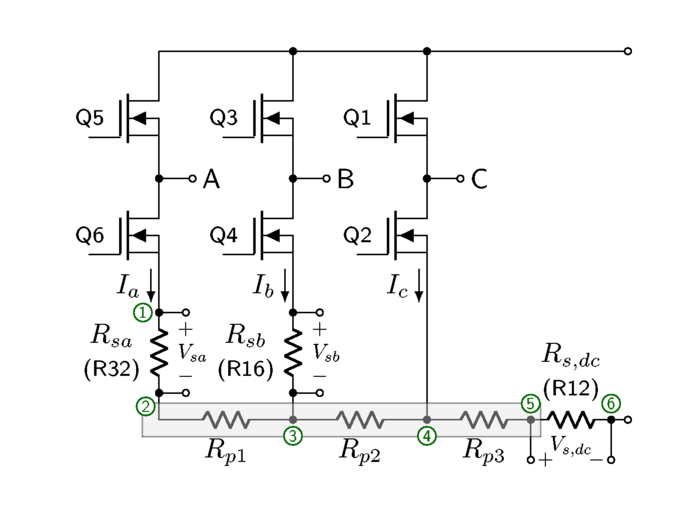
Figure 7.2 Three-phase bridge in MCLV-2, real circuit with proper layout
Unfortunately there were some layout errors in the MCLV-2 board. Kelvin connections were used, but were shorted together in signal traces, so the voltage drops along these parasitic resistances do affect the current measurements, and can effectively be modeled as shown in Figure 7.3, where the shorted node ⑦ is used for the common terminal in all three current sensing circuits.
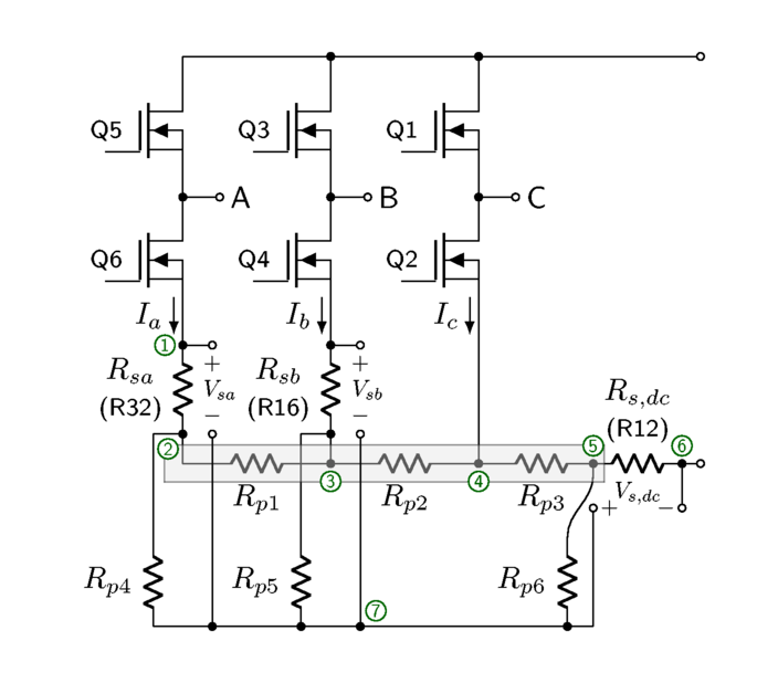
The approximate values of these trace resistances at room temperature (measured by connecting a current-limited power supply to various pairs of circuit nodes, and measuring current delivered by the power supply and voltages at various points, e.g. putting current into node ① on sense resistor \(R_{sa}\) and out of node ⑥ on sense resistor \(R_{s,dc}\), in order to measure \(R_{p1}\), \(R_{p2}\), and \(R_{p3}\)) are
- \(R_{p1} \approx 3.3\ \text{m}\Omega\)
- \(R_{p2} \approx 2.9\ \text{m}\Omega\)
- \(R_{p3} \approx 0.3\ \text{m}\Omega\)
- \(R_{p4} \approx 90\ \text{m}\Omega\)
- \(R_{p5} \approx 58\ \text{m}\Omega\)
- \(R_{p6} \approx 63\ \text{m}\Omega\)
This effectively means the voltage \(V_{7}\) at node ⑦ is a weighted average of the three voltages \(V_a\) at node ②, \(V_b\) at node ③, and \(V_{dc}\) at node ⑤: \(V_7 = K_aV_a + K_bV_b + K_{dc}V_{dc}\). Test currents were also used to measure the approximate weights \(K_a \approx 0.25\), \(K_b \approx 0.39\), and \(K_{dc} \approx 0.36\).
If we sample currents when all the lower switches are on, and \(I_a + I_b + I_c\) is 0, then the voltage drop across \(R_{p3}\) is 0, and the other two voltage drops are \(I_aR_{p1}\) and \((I_a + I_b)R_{p2}\). We can analyze the circuit to determine the impact on current sensing, and if we write the sense resistors as a nominal resistance \(R_s\) with a tolerance, \(R_{sa} = R_s(1+\delta_a)\) and \(R_{sb} = R_s(1+\delta_b)\), we can simplify the result to the following :
or in matrix form:
with
In other words, if the sense resistors had no tolerance error (\(\delta_a = \delta_b = 0\)) then \(\mathbf{K} \approx \begin{bmatrix}1.141 & 0.042 \cr 0.009 & 1.042 \end{bmatrix}\).
The compensation gain would be \(\mathbf{K}_\text{comp} \, = \, \mathbf{K}^{-1} \, \approx \begin{bmatrix}\phantom{-}0.877 & -0.035 \cr -0.008 & \phantom{-}0.960\end{bmatrix}\) for the nominal values.
This is essentially consistent with lab measurements putting in known currents into phase A and B and measuring the digitized ADC values; one set of those measurements produced an empirical estimate of \(\mathbf{K}_\text{empirical}\, = \begin{bmatrix}1.150 & 0.044\cr 0.012 & 1.048\end{bmatrix}\).