
4.9. Hardware Abstraction Layer (HAL)
The HAL is used by MCAF to decouple all knowledge of device-specific hardware registers, via well-known function calls. The HAL is made up of two layers: MPLAB® Code Configurator (MCC) layer and HAF layer. The MCC layer is the base layer where device-specific hardware registers are abstracted out into a series of peripheral driver APIs. The HAF layer then calls functions in the MCC layer to abstract out device specific functionality, enabling the higher level MCAF layers to be device-independent.
As long as the HAL function names and semantics are preserved, the HAL component can be swapped out and replaced with an alternative implementation.
4.9.1. Hardware-Related Behavior
Certain aspects of MCAF utilize the functions provided by the HAL, but the choice of behavior lies within MCAF. Some of these choices have been made to facilitate portability between devices that have different underlying peripheral mechanisms.
Note: this portability comes at a cost — each series of microcontrollers has certain peripheral usage patterns that are optimal but which may not translate well across different series.
Customers for whom CPU or peripheral performance is a severe constraint that takes precedence over portability and maintainability, should consider modifying the HAL as necessary to meet those constraints. Microchip does not recommend this approach unless absolutely necessary.
4.9.1.1. Interrupt priorities
The majority of MCAF code is executed in several different interrupt service routines. The following interrupts, listed from highest to lowest priority, are used by MCAF. See the scheduling requirements section for more information.
Main ADC ISR — Executes the state machine and several other critical MCAF components once every PWM period.
Single-channel ADC ISR — Samples the DC link current twice every PWM period. Only executed if single-channel current measurement is used.
Timer ISR — Executes the board service tasks and the main application periodically.
4.9.1.2. PWM outputs
PWM outputs for the three-phase bridge are set in one of three modes:
off — at device reset, and during severe faults, the bridge is turned off completely
“minimal impact” — when not applying voltage across the motor terminals (in certain states of the state machine), the upper transistors are turned off completely, but the lower transistors are turned on at a low duty cycle (typically 1-3%), to maintain charge in bootstrap gate drive capacitors. See
MCAF_SetPwmMinimalImpact()in the state_machine module.normal — when applying voltage across the motor terminals, all 6 of the transistors are switching, in three complementary pairs, one for each phase. Each phase has a dead-time between turn-off of one transistor and turn-on of the complementary transistor, to avoid shoot-through.
4.9.1.3. Overcurrent fault detection and clearing
MCAF requires a two phase fault clearing scheme to reset the latch circuitry. In order to clear the fault in Latched mode in dsPIC33EP devices, it is necessary to clear the interrupt flag and enable the fault mode at the next PWM cycle. Please refer to DS70645C p.14-101 for additional information.
Phase 1 occurs at current PWM cycle
33EP: Disable the fault latch mode
33CK: Clear the fault latch
Phase 2 occurs at the next PWM cycle
33CK & 33EP: Clear the fault interrupt flag
33EP: Enable the fault latch
4.9.1.4. Analog-to-digital conversion
Some of the ADC inputs have strict timing requirements, as shown in Table 4.8.
(At present, MCAF requires a fixed \(f_{PW\!M}\) = 20 kHz.)
Analog input |
Sampling frequency |
Timing requirements |
|---|---|---|
Motor currents (A,B,Sum) |
\(f_{PW\!M}/K\) |
Sample near the center of the PWM cycle(typically the start of center-aligned cycle). All samples should be complete within some small time Tskew. (Typically 1 μs or less) |
DC link voltage |
\(f_{PW\!M}/K\) |
K=1 or K=2 typical. (Minimizing K is preferred.) Otherwise, no strict timing requirements |
Potentiometer |
\(f_{PW\!M}/K\) |
Depends on the application; MCAF uses K=2. Otherwise, no strict timing requirements |
Given the above constraints, multiple ADC sample scheduling schemes can be used. The timing diagrams below show the sampling schedules of motor phase currents, DC link voltage, and potentiometer in both 33CK and 33EP. The ADC trigger source is selected by mapping any available PWM instance to Phase A in the board configuration file. This allows the selection of different PWM generators, for example PWM generator 2 or 3, to trigger the ADC by mapping it accordingly.
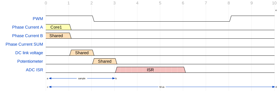
Figure 4.12 Suggested ADC Timing on dsPIC33CK devices with multiple ADC cores (horizontal axis not to scale)
Figure 4.12 shows an example of dsPIC33CK devices with multiple cores (such as the dsPIC33CK64MP105, and dsPIC33CK256MP508) sampling motor currents phase A and B simultaneously at the beginning of the center-aligned PWM cycle. After motor current phase B, with less than 1 μs between samples, the shared core sequentially samples the DC link voltage, potentiometer, and other ADC channels. At the end of the conversion sequence the interrupt is triggered and the ADC ISR executes.
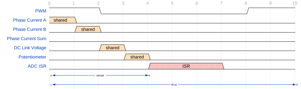
Figure 4.13 Suggested ADC Timing on dsPIC33CK devices with single ADC cores (horizontal axis not to scale)
Figure 4.13 shows an example of dsPIC33CK devices with a single ADC core (such as dsPIC33CK64MC105) sampling analog inputs: motor phase A and B currents, DC link voltage, potentiometer, sequentially, and any other ADC channels. At the end of the conversion sequence the interrupt is triggered and the ADC ISR executes.
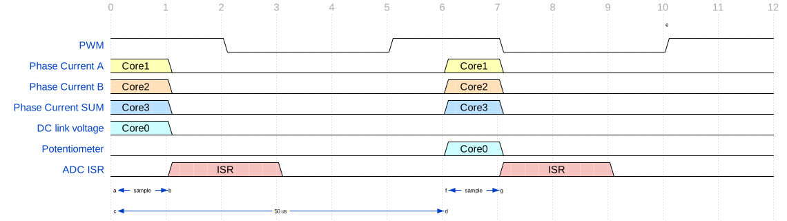
Figure 4.14 Suggested ADC Timing on dsPIC33EP devices (horizontal axis not to scale)
Figure 4.14 shows an example of dsPIC33EP256MC506 sampling all analog inputs simultaneously at the beginning of the center-aligned PWM cycle, with the exception of the potentiometer input. After analog inputs have been sampled and converted, this triggers the beginning of the ADC ISR. At the next center-aligned PWM cycle the shared ADC core is switched from sensing DC link voltage to sensing the potentiometer input. At the next PWM boundary, this cycle repeats.
4.9.1.4.1. Difference between 33EP and 33CK PWM modules and its implications on ADC operation
To measure the motor phase currents accurately, the ADC must sample during the low-side duty cycle pulse after the settling time. This allows enough time for current sense signal conditioning to settle and charge the ADC sampling capacitor before the low-side pulse has ended.
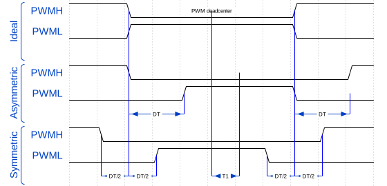
Figure 4.15 
Figure 4.15 shows the difference between symmetric and asymmetric dead time. In symmetric dead time, high-to-low transitions are advanced by DT/2 and low-to-high transitions are delayed by DT/2. In asymmetric dead time, low-to-high transitions are delayed by DT. This figure also shows that in asymmetric dead time insertion, the PWM dead-center event is delayed by T1.
- dsPIC33EP:
Implements symmetric dead time in PWM module
Due to symmetric dead time, the beginning of the center-aligned cycle is aligned with the center of the low-side pulse.
No delay is required to ensure sampling/conversion occurs in the middle of the low-side pulse.
- dsPIC33CK:
Implements asymmetric dead time in PWM module
Due to asymmetric dead time the beginning of the center-aligned cycle is slightly ahead of the center of the low-side pulse.
Add a small delay of half the dead time to the ADC trigger to ensure sampling/conversion occurs in the middle of the low-side pulse.
4.9.1.5. PWM update options
For center-aligned PWM, there are several choices that determine when updates to the PWM duty cycle registers are actually loaded into the PWM generator for use.
These choices usually include the following:
immediate update — duty cycle register updates are loaded into the PWM generator immediately. This has the lowest additional delay, but can cause extra output transitions (for example, if the duty cycle registers are updated from an older larger duty cycle, to a newer smaller duty cycle, after the older duty cycle has already caused a low-to-high transition, but before the newer duty cycle would cause a low-to-high transition) or fall within known errata of the PWM module. Immediate update is not recommended for use with MCAF.
single update (single synchronous update) — duty cycle register updates are loaded into the PWM generator at the start of the center-aligned PWM period. This creates only one opportunity per PWM cycle for control loops to update the duty cycle.
double update (double synchronous update) — duty cycle register updates are loaded into the PWM generator both at the start and the center of the center-aligned PWM period. This creates two opportunities per PWM cycle for control loops to update the duty cycle.
The choice of update creates an effective delay in the current control loop timing. The critical metric is the sample-to-update delay \(T_{su}\), which measures the time between the instant that information is available from ADC sampling, until a new set of PWM duty cycles is loaded into the PWM generator. Single update and double update are shown in Figure 4.16. Double-update PWM allows for a minimum delay \(T_{su}\) of one half PWM cycle. Single-update PWM allows for a minimum delay \(T_{su}\) of one full cycle. The actual delay depends on how quickly the control loop executes the critical code between ADC sampling and PWM duty cycle register update.
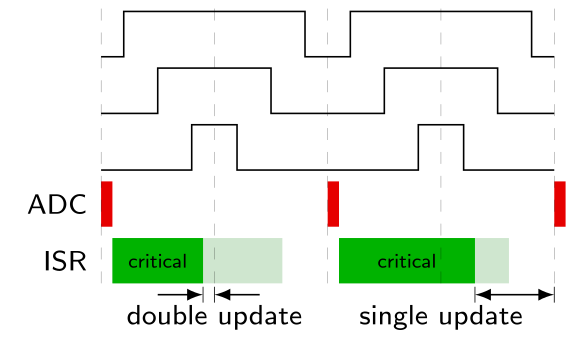
Figure 4.16 Single update and double update. The dashed lines represent opportunities for PWM generator update.
Double update is recommended for MCAF, in general, to reduce sample-to-update delay, but some control methods require other PWM update options. ZS/MT requires single update in Center Aligned PWM Mode. For other estimators, single-channel current measurement requires single update in Dual Edge Center Aligned PWM Mode, and for dual-channel or triple-channel current measurement, Double Update Center Aligned PWM Mode is configured to reduce sample-to-update delay.
Note: In dsPIC33E devices double update is enabled by default and does not require or allow any change in peripheral configuration. For dsPIC33E please check the device errata. Earlier silicon revisions for some devices implement the single-update behavior rather than double-update behavior.
4.9.1.6. Board service module
The board service module in MCAF works with Hardware Access Functions (HAF) in the HAL in order to provide MCAF with board-level functionality. It provides two main board-related features: a board handler and a PWM bootstrap charging routine.
4.9.1.6.1. Board handler
The board handler includes interfaces to configure and execute a board service process. The board service process uses a timer to periodically handle board level services. Working with appropriate HAL interfaces, the board handler provides services to push buttons, potentiometer, and configurable PWM drivers (if available) to applications such as the sample application or custom applications.
4.9.1.6.2. PWM bootstrap charging routine
The PWM bootstrap charging routine includes interfaces to initialize and execute the PWM bootstrap charging process. The routine begins by turning the high-side transistors off and setting the low-side transistors to 0% duty cycle. Then the PWM bootstrap charging routine delays a preset number of PWM cycles before beginning to charge the bootstrap capacitors. During the process, the PWM bootstrap capacitors are sequentially charged at a controlled rate (see errata). The process begins by switching the phase A low-side transistor at a low duty cycle for a short time, before proceeding with phase B for a short time, and then phase C:
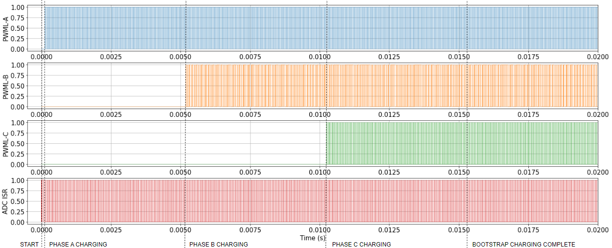
Figure 4.17 PWM low-side signals during bootstrap charging routine.
4.9.2. Implementation
4.9.2.1. MCC integration
Prior to MCAF R3, generated code was not integrated with MCC; MCAF provided its own HAL completely.
4.9.2.1.1. MCAF R3
In MCAF R3, the following items have been removed from MCAF and made the responsibility of MCC:
Configuration bits
Oscillator setup
Some aspects of the MCC system module are still present in MCAF. Both MCC and MCAF code executes; the MCAF code runs later and overrides any settings from MCC. The following areas are handled both by MCC and MCAF:
GPIO configuration
Interrupt initialization
CORCON initialization
This overlap is temporary, and these areas are planned to be shifted fully to MCC.
Other modules such as ADC and PWM are configured solely by MCAF, and will be shifted to MCC in a future version of MCAF.
4.9.2.1.2. MCAF R4
In MCAF R4, the following items have been removed from MCAF and made the responsibility of MCC:
GPIO configuration
Interrupt module
CORCON initialization
PWM module
ADC module
Timer module
UART module
DMA module
Watchdog module
LEDs module
Switches module
Pin Management (partially)
MCC handles all peripheral initialization, pin initialization, pin management, and is the base layer for interacting with hardware. Currently, because MCC does not yet support QEI, pin management cannot be fully handled by MCC alone. First, the MCC system module configures all peripherals including device pin management. Then, after the MCC system module is done with configuration, MCAF pin management is run as well to initialize QEI pins. The QEI module is fully handled by MCAF and will be shifted to MCC when QEI support is available in MCC for 16-bit devices.
Most hardware access actions occur through the HAF layer but a few calls to the MCC peripheral layer are made directly from the MCAF application. In the future, all hardware access will be delegated to the HAF layer. This is to avoid coupling between the MCAF application and MCC.
HAL_InterruptVectorNumberGet() is a function that has been added to the HAF layer. This
function retrieves the interrupt vector number, and does not directly go through MCC to do so.
More information about MCC configuration in MCAF is available in the MCC Peripheral documentation.
4.9.2.1.3. MCAF R5
Added support for dsPIC33CK256MP508.
All peripheral and hardware related functions called by MCAF are made through the Hardware Access Functions layer.
MCAF requires certain instances of peripherals. Required instances are: PWM, ADC1, TMR1, SCCP1-TMR/TMR2, UART1 and QEI1
MCC handles most peripheral generated code except for QEI and clearing of the fault interrupt status bits.
4.9.2.1.4. MCAF R6
Added support for dsPIC33CK64MP105, and dsPIC33CK64MC105.
MCC now handles all of the peripheral generated code except for QEI.
Board service module restructured to split into PWM bootstrap charging and board handler sections
4.9.2.1.5. MCAF R7
- Added support for both MCC Melody and MCC Classic.
MCC Melody is supported only for the dsPIC33CK family of devices.
MCC Classic is supported only for the dsPIC33EP family of devices.
MCC Melody handles all of the peripheral generated code, including QEI. When using MCC Classic, MCAF provides QEI code.
Interrupt priorities used by MCAF are summarized in Table 4.9.
Table 4.9 ISR priorities for MCAF¶ ISR type
MCC Classic
MCC Melody
Main ADC
4
6
Single-channel ADC
N/A
5
Timer
4
4
4.9.2.1.6. MCAF R9
Prior to MCAF R9 the ADC trigger was hardcoded to PWM generator 1. Since MCAF R9, customize the ADC trigger source, if needed, by mapping any available PWM instance to Phase A in the board configuration file.
4.9.2.2. HAL errata
MCAF_BootstrapChargeStepIsr()includes a soft-start sequence intended to slowly turn on duty cycle and reduce gate drive power supply loading in order to charge up bootstrap capacitors. This sequence starts with duty cycles that are too low, and may produce runt pulses with certain gate drivers. (DB_MC-978; Applicability: MCAF R2 – R6)