Hardware Architecture
This section describes the hardware architecture produced by SmartHLS.
Circuit Topology
Each C/C++ function corresponds to a hardware module in Verilog. For instance, if we have a software program with the following call graph:
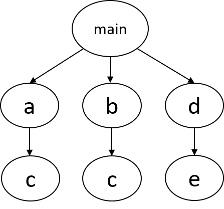
where main calls a, b, and d, each of which calls c, c, and e, respectively.
Notice that function c is called by both a and b.
One way to create this system in hardware is to instantiate one module within
another module, in a nested hierarchy, following how the functions are called in software:

This architecture is employed by some of the other HLS tools, but it can create an unnecessary
replication of hardware. Notice how module c has to be created twice, since the function c is called from different parent functions.
In SmartHLS, we instantiate all modules at the same level of hierarchy, and automatically create the necessary interconnect
to connect them together.
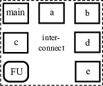
This prevents modules from being unnecessarily replicated, saving area.
The hardware system may also use a functional unit (denoted as FU in the figure),
such as a floating-point unit, which is also created at the same level.
This architecture also allows such units, which typically consume a lot of area,
to be shared between different modules.
Note
For a small function, or for a function that is only called once in software, SmartHLS may decide to inline the function into its parent function to improve performance.
Any inlined function is included as part of its parent function, so there will not be a separate module in the Verilog for the inlined function.
Thus you may not find all the software functions in the generated hardware.
Threaded Hardware Modules
When threads are used in software, SmartHLS automatically compiles them to concurrently executing modules.
This is synonymous to how multiple threads are compiled to execute on multiple processor cores in software.
By default, each thread in software becomes an independent hardware module.
For example, forking three threads of function a in software creates three concurrently executing instances of module a in hardware.
Memory Architecture
SmartHLS stores any arrays (local or global) and global variables in a memory. We describe below what type of memories they are, as well as where the memories are stored.
In SmartHLS, there exists four hierarchies of memories: 1) Local memory, 2) shared-local memory, 3) aliased memory, and 4) I/O memory. Local, shared-local, and aliased memories exist in the generated hardware. I/O memories are data that are inputs/output to/from the generated hardware. They exist outside of the generated hardware (SmartHLS does not instantiate memories for them), where top-level memory interfaces are created for them.
Local Memory
SmartHLS uses points-to analysis to determine which memories are used by which functions. If a memory is determined to be used by a single function, where the function is to be compiled to hardware, that array is implemented as a local memory. A local memory is created and connected directly inside the module that accesses it.
Local memories have a latency of 1 clock cycle by default. The local memory latency can be changed with the set_operation_latency Tcl parameter.
Aliased Memory
There can be cases where a pointer can point to multiple arrays, causing pointer aliasing. These pointers need to be resolved at runtime. We designate the memories that such a pointer can refer to as aliased memories, which are stored in a memory controller (described below). A memory controller contains all memories that can alias to each other, and allows memory accesses to be steered to the correct memory at runtime. There can be multiple memory controllers in a system, each containing a set of memories that alias to each other.
Aliased memories have a latency of 2 clock cycles. The aliased memory latency can be changed with the set_operation_latency Tcl parameter.
Memory Controller
The purpose of the memory controller is to automatically resolve pointer ambiguity at runtime. The memory controller is only created if there are aliased memories. The architecture of the memory controller is shown below:
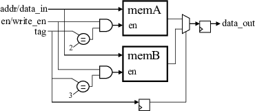
For clarity, some of the signals are combined together in the figure. Even though the figure depicts a single-ported memory, all memories are dual-ported by default, unless only a single memory access is needed per cycle, in which case it will be single-ported memory. The memory controller steers memory accesses to the correct RAM, by using a tag, which is assigned to each aliased memory by SmartHLS. At runtime, the tag is used to determine which memory block to enable, with all other memory blocks disabled. The same tag is used to select the correct output data between all memory blocks.
I/O Memory
Any memory that is accessed by both the software testbench (parent functions of the top-level function) and hardware functions (the top-level functions and its descendants) becomes an I/O memory. These are any non-constant arguments for top-level function or global variables that are accessed by both the software testbench and hardware functions. I/O memories become memory interfaces of the top-level module for the generated hardware, where no actual memories are instantiated within the generated hardware for them. For more information on interfaces, please refer to Top-Level RTL Interface.
Memory Implementation
By default, each local, shared-local, and aliased memories are stored in a separate dual-ported on-chip RAM, where each RAM allows two accesses per clock cycle. All local memories can be accessed in parallel. All shared-local memories can be accessed concurrently when there are no accesses to same memory in the same clock cycle. If there are concurrent accesses to the same RAM, arbitration logic handles the contention automatically and stalls the appropriate modules. All independent memory controllers can also be accessed in parallel, but aliased memories which belong to the same memory controller will be accessed sequentially.
Memory Optimizations
SmartHLS automatically stores each single-element global variable (non-array) in a set of registers, rather than a block RAM, to reduce memory usage and improve performance. A block RAM has a minimum read latency of 1 clock cycle, where a register can be read in the same clock cycle (0 cycle latency). For small arrays, SmartHLS may decide to split them up and store individual elements in separate registers. This allows all elements to be accessed at the same time. If an array is accessed in a loop, and the loop is unrolled, SmartHLS also may decide to split up the array.
If only up to a single memory accessed is needed per cycle for a memory, SmartHLS will instantiate a single-ported RAM, otherwise a dual-ported RAM will be used. If a memory is only ever read from, SmartHLS will convert the memory to a read-only memory (ROM), even if the corresponding array is not declared as a constant in software. If a memory is not accessed at all, SmartHLS will automatically optimize away the memory.
Interfaces
Please refer to the Top-Level RTL Interface section for a detailed description on the interfaces that are created by SmartHLS.
SmartHLS Reference SoC
Note
This feature is specific to SmartHLS SoC early access program (EAP), and requires a separate SmartHLS EAP license. If you are interested in participating in the EAP, please email SmartHLS@microchip.com.
This section describes the architecture of the reference SoC that can be optionally generated by SmartHLS for AXI4 target/initiator-compatible accelerators. This reference SoC is targeted for PolarFire SoC Icicle Kit, and contains:
The Icicle Kit’s Hardened Microprocessor Sub-System (MSS).
Any accelerators created from the user’s project.
A fabric AXI4 interconnect, connecting the MSS and accelerators.
A diagram of the reference SoC architecture is shown below:
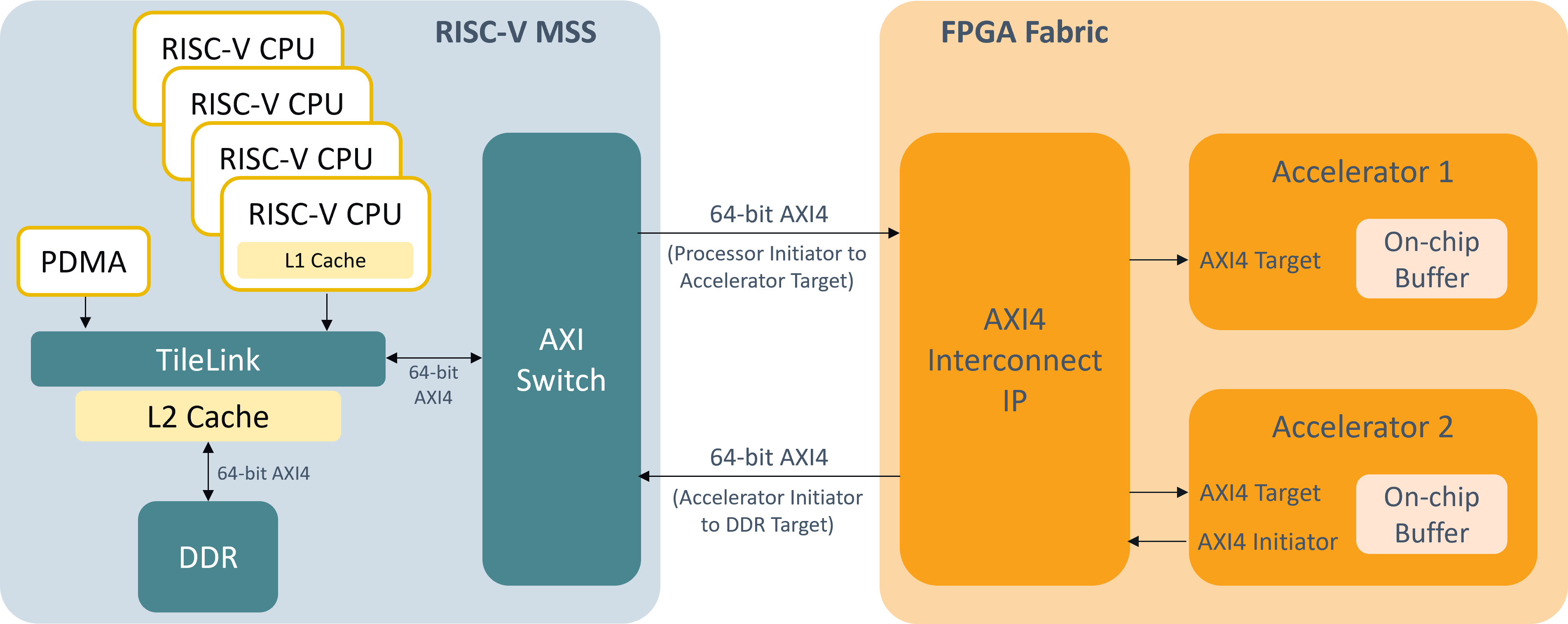
On the left-hand side is the Microprocessor Sub-System (MSS). This is a hardened module on the Icicle Kit, containing four RISC-V cores, DDR memory, a hardened DMA controller, and related components. MSS components are connected internally with a TileLink switch, and interface with the FPGA fabric with both an AXI4 Initiator and AXI4 Target interface over an AXI switch. For more details on the MSS, please see the PolarFire SoC MSS Technical Reference Manual.
On the right-hand side of the diagram is the FPGA fabric. An AXI4 interconnect on the fabric connects the AXI4 interface from the MSS to one or more SmartHLS-generated accelerators. Each accelerator has an AXI4 Target interface, and depending on the specified interface type, can have an AXI4 Initiator interface as well. Additionally, each accelerator has an on-chip memory buffer for each pointer argument, which acts as local storage for the argument data, which is accessible to the MSS/DDR via AXI transactions and is directly connected to the hardware accelerator.
An example accelerator architecture diagram is shown below. In the figure, the accelerator has three pointer arguments, argA, argB, and argC. The arguments, argA and argB, are transferred to on-chip memory buffers via an AXI4 Target interface. The accelerator directly accesses data for argC via an AXI4 Initiator interface. The interfaces are created based on the pragma, #pragma HLS interface argument(<arg_name>) type(axi_target/axi_initiator) (see AXI4 Target Interface for Pointer Argument, AXI4 Initiator Interface for Pointer Argument). For details on the different data transfer methods for the AXI Target/Initiator arguments, see :ref:soc_data_transfer_methods.
